- 您现在的位置:买卖IC网 > Sheet目录3841 > PIC18F86K22-I/PTRSL (Microchip Technology)MCU PIC 64K FLASH XLP 80TQFP
2009-2011 Microchip Technology Inc.
DS39960D-page 23
PIC18F87K22 FAMILY
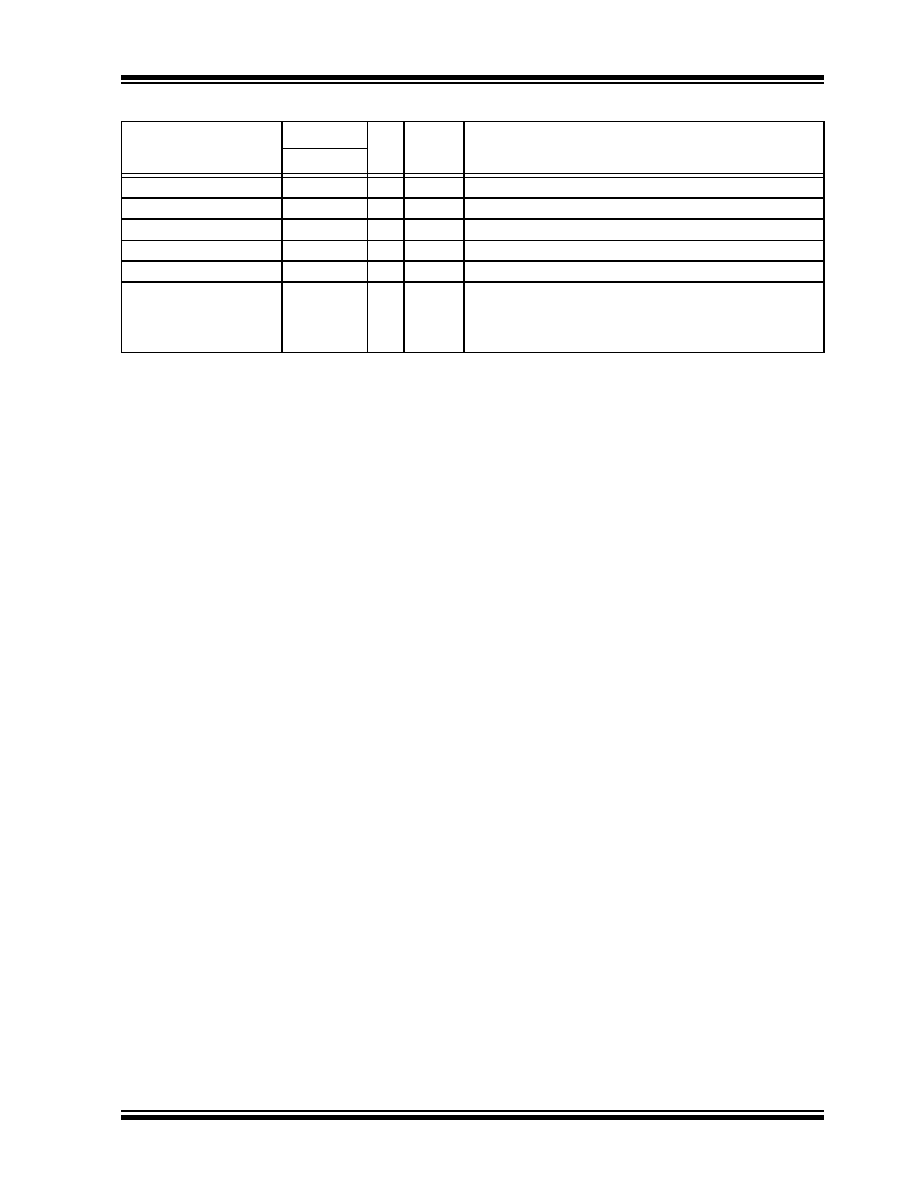
VSS
9, 25, 41, 56
P
—
Ground reference for logic and I/O pins.
VDD
26, 38, 57
P
—
Positive supply for logic and I/O pins.
AVSS
20
P
—
Ground reference for analog modules.
AVDD
19
P
—
Positive supply for analog modules.
ENVREG
18
I
ST
Enable for on-chip voltage regulator.
VDDCORE/VCAP
VDDCORE
VCAP
10
P—
Core logic power or external filter capacitor connection.
External filter capacitor connection (regulator
enabled/disabled).
TABLE 1-3:
PIC18F6XK22 PINOUT I/O DESCRIPTIONS (CONTINUED)
Pin Name
Pin Number Pin
Type
Buffer
Type
Description
QFN/TQFP
Legend:
TTL = TTL compatible input
CMOS = CMOS compatible input or output
ST = Schmitt Trigger input with CMOS levels
Analog = Analog input
I
= Input
O
= Output
P
= Power
OD
= Open-Drain (no P diode to VDD)
I2C= I2C/SMBus
Note 1:
Default assignment for ECCP2 when the CCP2MX Configuration bit is set.
2:
Alternate assignment for ECCP2 when the CCP2MX Configuration bit is cleared.
3:
Not available on PIC18F65K22 and PIC18F85K22 devices.
4:
The CC6, CCP7, CCP8 and CCP9 pin placement depends on the setting of the ECCPMX Configuration bit
(CONFIG3H<1>).
发布紧急采购,3分钟左右您将得到回复。
相关PDF资料
PIC16C63A-04I/SP
IC MCU OTP 4KX14 PWM 28DIP
PIC16C63A-04I/SO
IC MCU OTP 4KX14 PWM 28SOIC
52559-2270
CONN FFC 22POS .5MM VERT ZIF SMD
52559-1870
CONN FFC 18POS .5MM VERT ZIF SMD
DSPIC33EP64MC506-I/PT
IC DSC 16BIT 64KB FLASH 64TQFP
52745-1896
CONN FFC 18POS .5MM R/A ZIF SMD
PIC16LC622-04/P
IC MCU OTP 2KX14 COMP 18DIP
PIC16LF84A-04/P
IC MCU FLASH 1KX14 EE 18DIP
相关代理商/技术参数
PIC18F86K22-I/PTRSL
制造商:Microchip Technology Inc 功能描述:IC MCU 8BIT 64K FLASH 80TQFP ((NW)) 制造商:Microchip Technology Inc 功能描述:IC, 8BIT MCU, PIC18F, 16MIPS, TQFP-80
PIC18F86K22T-I/PT
功能描述:8位微控制器 -MCU 64kB Flash 4kB RAM
RoHS:否 制造商:Silicon Labs 核心:8051 处理器系列:C8051F39x 数据总线宽度:8 bit 最大时钟频率:50 MHz 程序存储器大小:16 KB 数据 RAM 大小:1 KB 片上 ADC:Yes 工作电源电压:1.8 V to 3.6 V 工作温度范围:- 40 C to + 105 C 封装 / 箱体:QFN-20 安装风格:SMD/SMT
PIC18F86K22T-I/PTRSL
功能描述:8位微控制器 -MCU 64KB Flash 4KB RAM nanoWatt XLP GP RoHS:否 制造商:Silicon Labs 核心:8051 处理器系列:C8051F39x 数据总线宽度:8 bit 最大时钟频率:50 MHz 程序存储器大小:16 KB 数据 RAM 大小:1 KB 片上 ADC:Yes 工作电源电压:1.8 V to 3.6 V 工作温度范围:- 40 C to + 105 C 封装 / 箱体:QFN-20 安装风格:SMD/SMT
PIC18F86K90-E/PT
功能描述:8位微控制器 -MCU 64KB Flash 4KB RAM LCD
RoHS:否 制造商:Silicon Labs 核心:8051 处理器系列:C8051F39x 数据总线宽度:8 bit 最大时钟频率:50 MHz 程序存储器大小:16 KB 数据 RAM 大小:1 KB 片上 ADC:Yes 工作电源电压:1.8 V to 3.6 V 工作温度范围:- 40 C to + 105 C 封装 / 箱体:QFN-20 安装风格:SMD/SMT
PIC18F86K90-I/PT
功能描述:8位微控制器 -MCU 64kB Flash 4kB RAM LCD
RoHS:否 制造商:Silicon Labs 核心:8051 处理器系列:C8051F39x 数据总线宽度:8 bit 最大时钟频率:50 MHz 程序存储器大小:16 KB 数据 RAM 大小:1 KB 片上 ADC:Yes 工作电源电压:1.8 V to 3.6 V 工作温度范围:- 40 C to + 105 C 封装 / 箱体:QFN-20 安装风格:SMD/SMT
PIC18F86K90-I/PTRSL
功能描述:8位微控制器 -MCU 64KB 4KB RAM 16MIPS nanoWatt XLP LCD 5V RoHS:否 制造商:Silicon Labs 核心:8051 处理器系列:C8051F39x 数据总线宽度:8 bit 最大时钟频率:50 MHz 程序存储器大小:16 KB 数据 RAM 大小:1 KB 片上 ADC:Yes 工作电源电压:1.8 V to 3.6 V 工作温度范围:- 40 C to + 105 C 封装 / 箱体:QFN-20 安装风格:SMD/SMT
PIC18F86K90T-I/PT
功能描述:8位微控制器 -MCU 64kB Flash 4kB RAM LCD
RoHS:否 制造商:Silicon Labs 核心:8051 处理器系列:C8051F39x 数据总线宽度:8 bit 最大时钟频率:50 MHz 程序存储器大小:16 KB 数据 RAM 大小:1 KB 片上 ADC:Yes 工作电源电压:1.8 V to 3.6 V 工作温度范围:- 40 C to + 105 C 封装 / 箱体:QFN-20 安装风格:SMD/SMT
PIC18F86K90T-I/PTRSL
功能描述:8位微控制器 -MCU 64KB 4KB RAM 16MIPS nanoWatt XLP LCD 5V RoHS:否 制造商:Silicon Labs 核心:8051 处理器系列:C8051F39x 数据总线宽度:8 bit 最大时钟频率:50 MHz 程序存储器大小:16 KB 数据 RAM 大小:1 KB 片上 ADC:Yes 工作电源电压:1.8 V to 3.6 V 工作温度范围:- 40 C to + 105 C 封装 / 箱体:QFN-20 安装风格:SMD/SMT